All Semilab's MCV systems are equipped with automated, full hand-off, mercury handling system to increase safety and reliability. The user friendly software environment controls the measurements and also offers a great flexibility for detailed analysis of the measured structures. Full map capability up to 12"/300 mm. All features listed, including optional ones, are compatible with both the manual MCV-530(L) and the automatic
MCV-2200/2500/3000/3000P systems.
Explore the entire carrier density and resistivity profile in all silicon semiconductor structures of device processing with this automated system. Measurement range covers state-of-the art application needs.
Gate dielectrics characterization and resistivity monitoring with site-based measurements
(typically 5 or 9 points per wafer according to SEMI standard testing patterns).
Specially designed probe ensures that no damage is done to the wafer, because the probe is not contaminating the wafer surfaces.
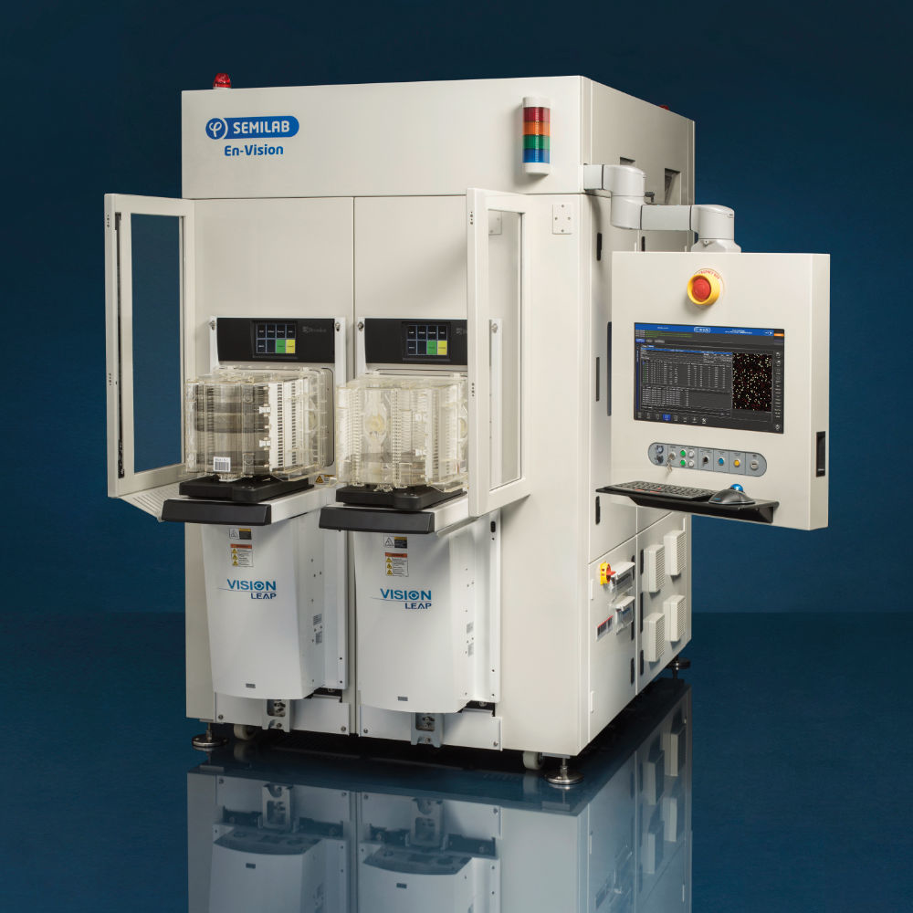
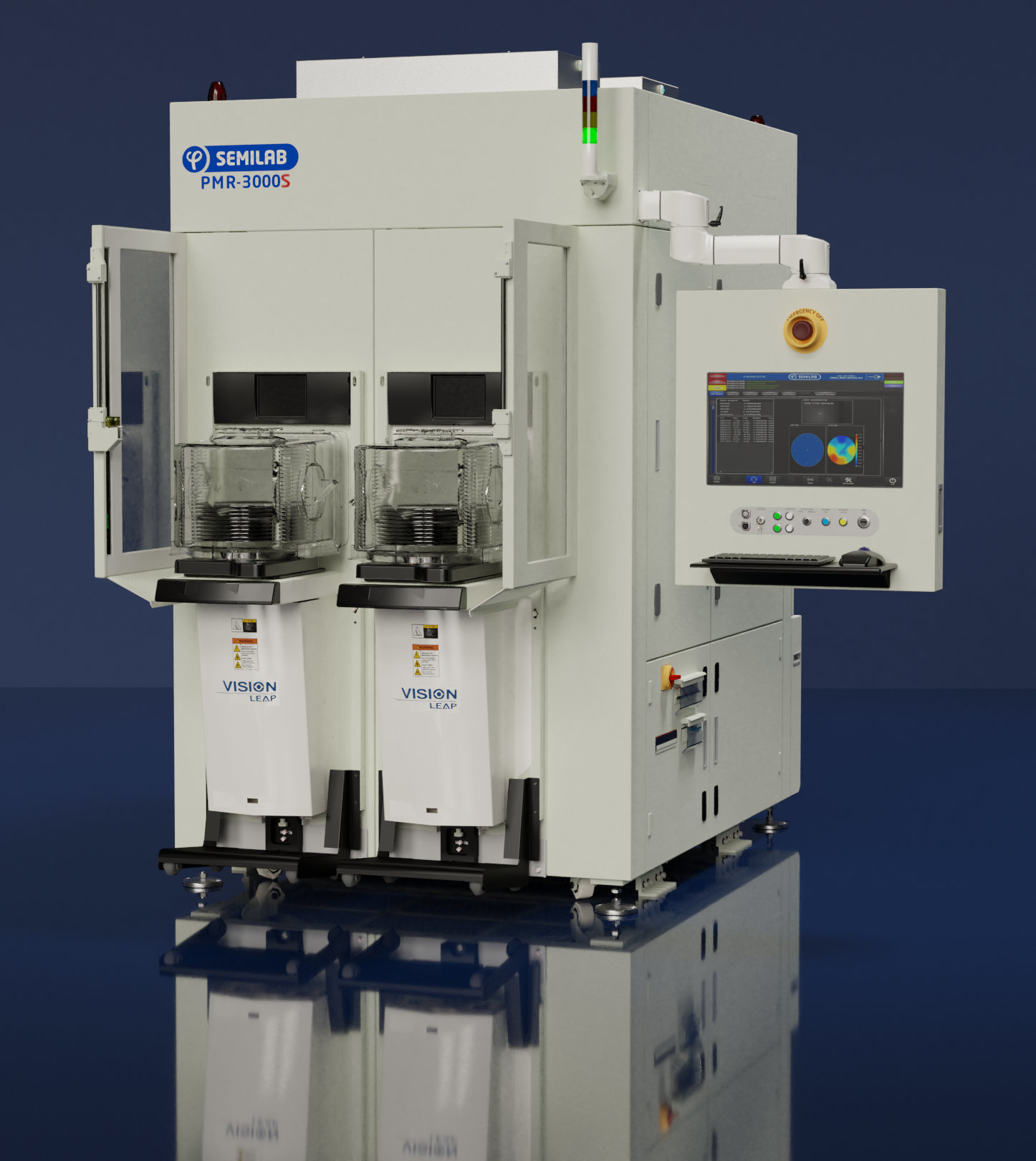
4 Point Probe (multiple heads) & Non-contact probes (JPV & EDDY) combined in one platform for better operability and long-term stability for wafer makers, device manufacturers and implanter suppliers.
Semilab’s QC platforms (Near Surface Doping Mappers) for epitaxial monitoring are the only non-contact, non-destructive, high throughput systems that can reliably map near surface doping on process wafers.