Go to text Go to main menu

Application

Display FPT (Flat Panel Tester)

  • Full-tone/Half-tone (Photoresist)
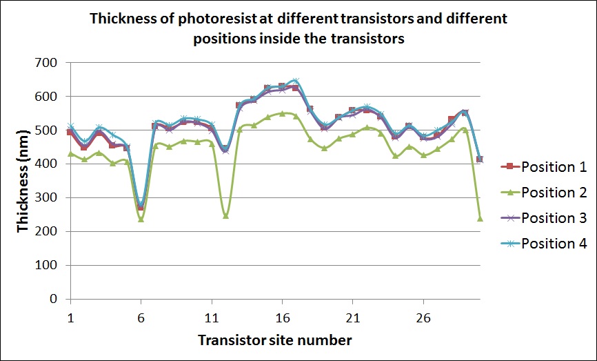
    Knowing photoresist thickness is very important at several steps in display manufacturing. Challenge could be the thick and UV sensitive layer as well as the measurement in very small (1-2 um) channel. Semilab can offer solution for both problems using metrology heads designed directly for this application.
    PRODUCT
  • Printed OLED sub-pixel characterization
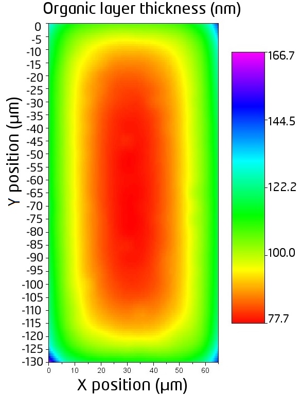
    Printing OLED is an attractive method for manufacturing devices containing organic layers due to its cost-effectiveness and relatively simple technique. However, in many cases, the uniformity of printed layers is significantly poorer compared to conventionally manufactured layers.

    Semilab has developed a metrology system that can accurately determine the complete thickness of the OLED structure within a single sub-pixel using just one measurement, and it does so in a matter of seconds. The lateral resolution can be as precise as 5 µm, allowing to finely adjust and optimize the printing process with great precision.
    PRODUCT
  • IGZO electrical characterization
    IGZO is considered one of the cutting-edge active layers in the display industry. However, even today, achieving the precise adjustment of the manufacturing process is essential to maintain the best layer properties.

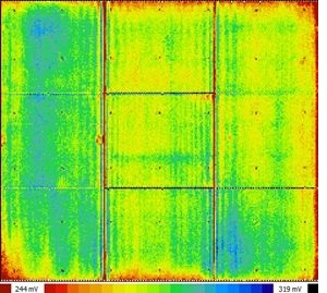
    By utilizing Semilab's µ-PCR and contact sheet resistance measurement techniques, one can efficiently map the panel at a reasonable speed. This mapping process can reveal any improper settings in the layer deposition process and open up opportunities for further optimization.

    µ-PCR can assess a parameter (amplitude) that is closely related to device mobility. Additionally, various other layer quality parameters (derived from the microwave response decay curve) can also be calculated using this method.
    PRODUCT
  • Sheet resistance measurement
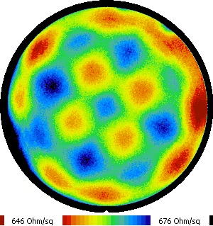
    The ion implantation process and subsequent annealing are typically monitored by measuring the sheet resistance of the implanted layer. Sheet resistance varies depending on factors such as dose, energy, and the level of implanted species that have become electrically active. Ultimately, it is the sheet resistance that plays a crucial role in determining device performance. Therefore, measuring sheet resistance serves as an excellent means to comprehensively monitor all aspects of an implantation process.

    The fundamental principle behind the JPV (Junction PhotoVoltage) method involves exciting the np or pn layer structure with light and then capturing the resulting junction photovoltage using a capacitive probe. The detected potential is influenced by factors like the sheet resistance of the implanted layer, junction capacitance, and resistance across the diode.
    PRODUCT
  • ELA process characterization (LTPS)
    Excimer Laser Annealing (ELA) plays a crucial role in the manufacturing of Low-Temperature Poly-Silicon (LTPS) layers, serving as a key process parameter. ELA influences several critical parameters of the layer and, consequently, the device itself, including crystallinity and mobility, among others. Semilab has developed a combination of metrology techniques that can readily determine the Optimal Energy Density (OED). This unique combination allows for distinguishing between the properties of two LTPS samples that have undergone annealing with very similar parameters. With this capability, fine-tuning the ELA process becomes a quick and straightforward task, eliminating the need for macro inspection and human decision-making.

    Additionally, our contact 6pp method can be used to determine sheet resistance
    PRODUCT
  • Bare glass
    The purity of the bare glass is a critical parameter for the success of all processes within the fabrication facility (fab). Semilab provides an integrated, user-friendly, and maintenance-free contact angle solution that can be seamlessly combined with (virtually) any other metrology tool.
    PRODUCT