The term "Bulk Micro Defects" (BMD) is commonly used to refer to oxygen precipitates within silicon. In reality, various imperfections within the silicon lattice create defects, and BMDs can encompass a range of imperfections including oxygen precipitates, voids, inclusions, and more.
BMDs are known by multiple names, often based on the issues they cause, their creation process, or their physical characteristics. Examples include terms like COPs (Crystal Originated Particles) and Grown-In Defects.
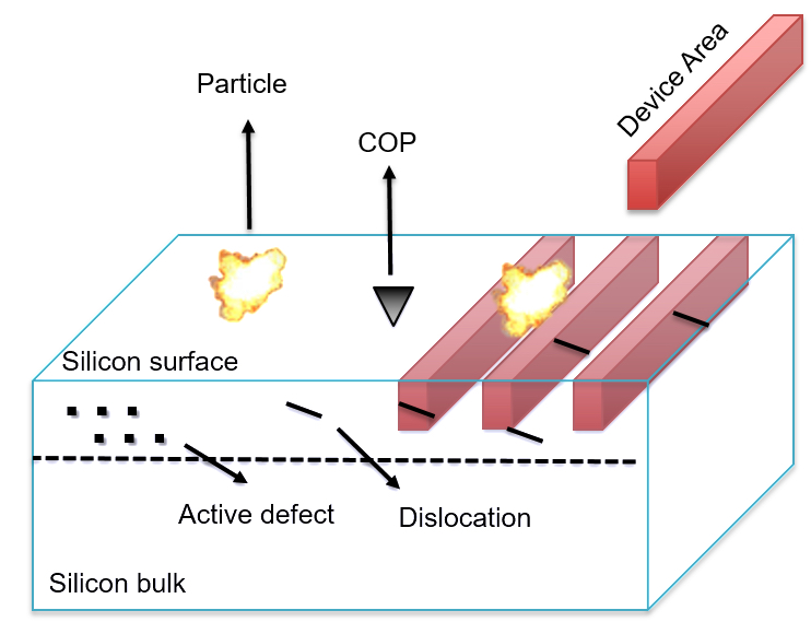
Dislocations can arise during crystal growth and also during thermal processing of wafers, especially during CMOS device manufacturing steps like epitaxial layer growth and implant annealing.
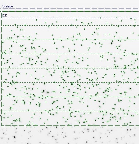
Imperfections within the semiconductor lattice and impurities create energy states within the bandgap, reducing carrier lifetime and increasing junction leakage. These imperfections also act as gettering sites, where impurities tend to accumulate. The profile of BMDs is often controlled through a complex series of high-temperature processes, creating a "denuded zone" as depicted in Figure 1. In this way, the surface silicon layer where MOS transistor action occurs remains free of oxygen precipitates, while the oxygen precipitates in the underlying silicon act as gettering sites to keep impurities away from the MOS transistors.
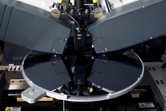
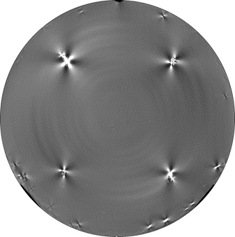
Infrared (IR) light can penetrate most semiconductor materials, and since BMDs alter the local optical properties of a semiconductor, they can be detected by illuminating a sample with IR light and observing it with an IR-sensitive camera.