Features and System specifications:
Benefits
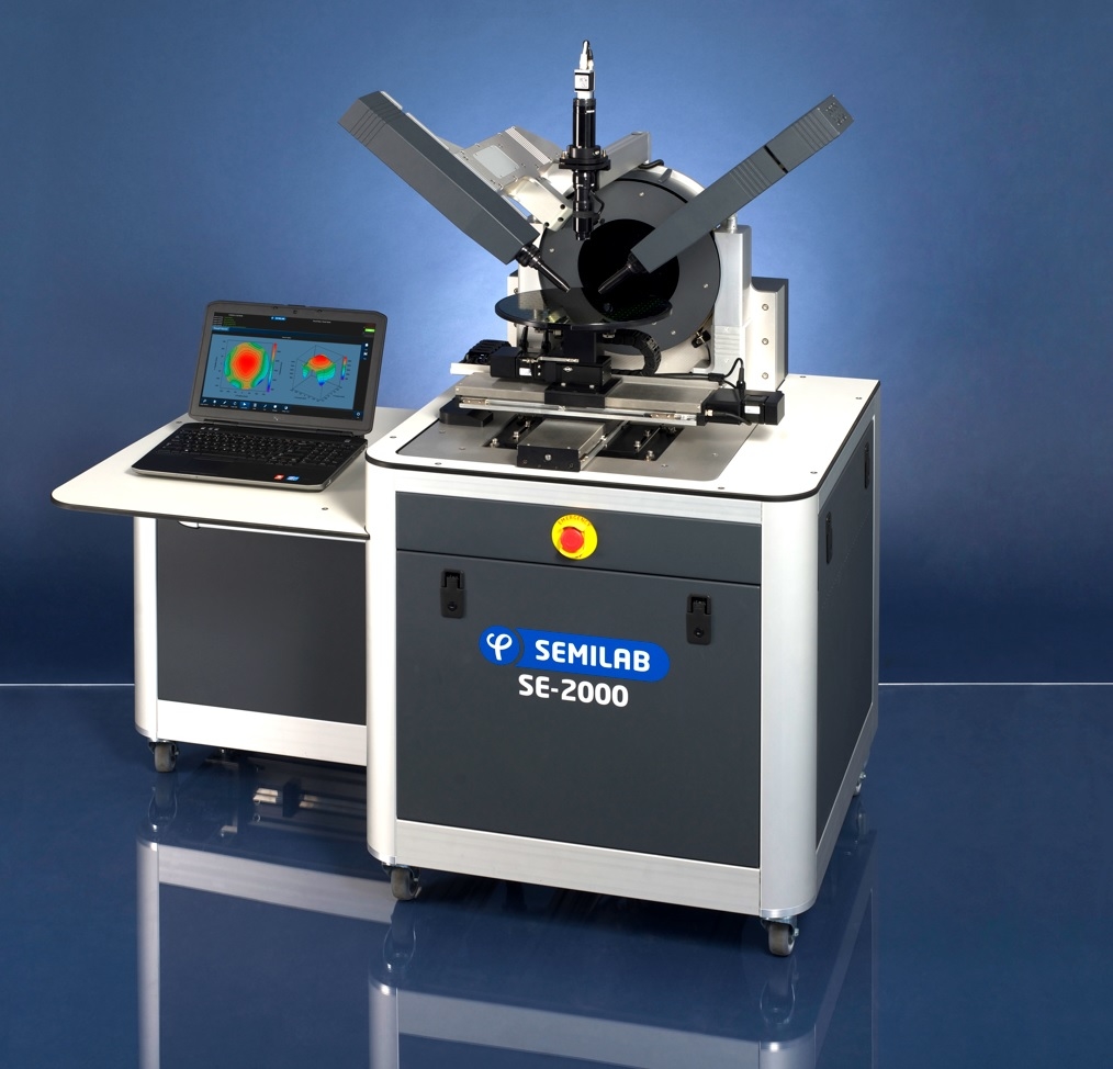
Non-destructive optical technique, based on measurement of the change of the polarisation state of light after reflection at non normal incidence on the surface to study.
It is a highly sensitive even for layer thickness below 1 nm
Extremely versatile technique: it gives acccess to numerous parameters which characterize multilayer structures (eg. layer thickness, refractive index, absorption, porosity).
Applications
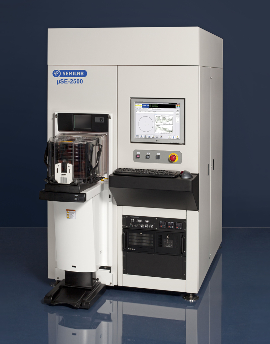
Thin film dielectric or semiconductor layer stack on solid polished surface substrate is the main target of applications.
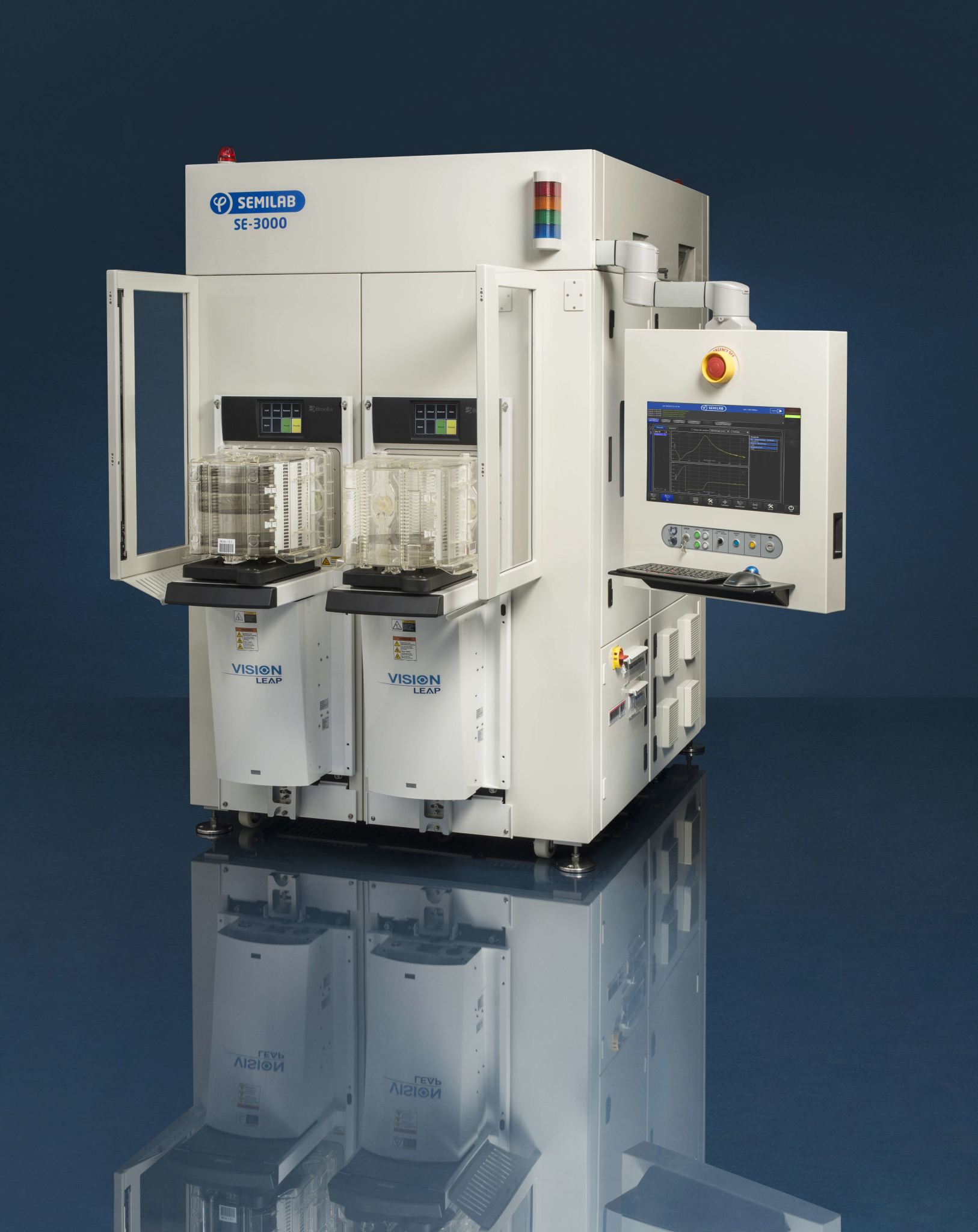
Pattern-capable Spectroscopic Ellipsometry
On high-performance silicon CMOS or III/V devices
After deposition and etch processes
Measurement capability of product wafers in <50μm patterned test areas
OLED display applications
Multilayer characterization
Thickness, n, k measurement
Thickness map within sub-pixels
More than Moore (MtM) industrial applications
Compound materials measurements:
AlGaN, GaN, GaAsOx,
SiGe, Poly-Si with Raman extension
Graphene, CNT
Periodic thick layers definition

